Recent advances in the preparation, control and measurement of atomic gases have led to new insights into the quantum world and unprecedented metrological sensitivities, e.g. in measuring gravitational forces and magnetic fields. The full potential of applying such capabilities to areas as diverse as biomedical imaging, non-invasive underground mapping, and GPS-free navigation can only be realised with the scalable production of efficient, robust and portable devices. We introduce additive manufacturing as a production technique of quantum device components with unrivalled design freedom and rapid prototyping. This provides a step change in efficiency, compactness and facilitates systems integration. As a demonstrator we present an ultrahigh vacuum compatible ultracold atom source dissipating less than ten milliwatts of electrical power during field generation to produce large samples of cold rubidium gases. This disruptive technology opens the door to drastically improved integrated structures, which will further reduce size and assembly complexity in scalable series manufacture of bespoke portable quantum devices.
The current expansion in the field of quantum technologies and in particular quantum sensors has given rise to notable strides forward in device sensitivities with applications ranging from satellite independent navigation to non-invasive biomedical imaging1,2. As demand for wider use of these instruments grows, it is imperative to develop robust low-footprint components to provide practical portable systems.
Recent work has focused on the exploitation of quantum phenomena in compact out-of-laboratory devices based on latest advances in micro-manufacturing technology including optical and electron beam lithography3, waveguide writing4 and reactive ion beam etching5. These developments have enabled integrated atom chip based systems6,7 and commercial development of complete systems on a vehicle payload scale8,9,10. Additive manufacturing (3D-printing) is a significant emerging technology capable of providing solutions to a range of problems due to the design freedoms11,12, the scalable production of individually bespoke components, and weight reduction it facilitates. In this work we demonstrate how this radically different manufacturing approach can be used to reach a step change in performance of practical quantum devices.
Atom-based quantum devices exploiting the properties of thermal vapours13, trapped cold atomic clouds14,15 and quantum degenerate gases16 have been demonstrated experimentally. Many attempts to reduce experimental demands in atom trapping have been considered including single-beam magneto-optical trap (MOT) designs based on conical17, pyramidal18,19 and tetrahedral20 diffraction-based reflectors to reduce optical equipment. Evolving atom chip technology is being pursued for small-scale field production1,21,22. Current miniaturised traps used for magnetic trapping within large integrated systems for Bose-Einstein condensate (BEC) production have been conventionally machined23 restricting scalability in manufacture.
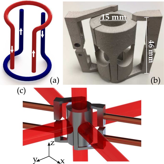
Here we present (Fig. 1) a 3D-printed centimetre scale demonstrator device providing a quantum resource through production of trapped cold atomic gases with unprecedented efficiency. While power consumption in the high-resistance chip conductors remains large, our approach in contrast allows us to trap tens of millions of atoms with merely 4 mW of electrical power consumption, and with magnetic field switching times under 10 μs. Our ultrahigh vacuum compatible device reliably produces a gas of up to 108 rubidium-87 atoms at a temperature of 20 μK fulfilling the demands of current experimental procedures19. We report here the design, manufacture and characterisation of the key performance properties of our prototype.


0 Comments