Abstract
There
has been an urgent need to eliminate toxic lead from the prevailing
halide perovskite solar cells (PSCs), but the current lead-free PSCs are
still plagued with the critical issues of low efficiency and poor
stability. This is primarily due to their inadequate photovoltaic
properties and chemical stability. Herein we demonstrate the use of the
lead-free, all-inorganic cesium tin-germanium triiodide (CsSn0.5Ge0.5I3)
solid-solution perovskite as the light absorber in PSCs, delivering
promising efficiency of up to 7.11%. More importantly, these PSCs show
very high stability, with less than 10% decay in efficiency after 500 h
of continuous operation in N2 atmosphere under one-sun
illumination. The key to this striking performance of these PSCs is the
formation of a full-coverage, stable native-oxide layer, which fully
encapsulates and passivates the perovskite surfaces. The native-oxide
passivation approach reported here represents an alternate avenue for
boosting the efficiency and stability of lead-free PSCs.
Introduction
The
promise of high efficiency and low cost has been propelling perovskite
solar cells (PSCs) research over the past decade or so. While the record power conversion efficiency (PCE) of PSCs is now approaching 24%
rivaling that of silicon-based solar cells, the state-of-the-art PSCs
employ lead-based organic–inorganic halide perovskite absorber
materials. The toxicity of lead associated with the lifecycle of these
PSCs is a serious concern, and it may prove to be a major hurdle in the
path toward their commercialization.
Thus, significant effort is being devoted toward the development of
low-cost, efficient lead-free PSCs. Several low-toxicity cations have
been proposed for replacing Pb(II) in halide perovskites, including
Ag(I), Bi(III), Sb(III), Ti(IV), Ge(II), and Sn(II).
Among these candidates, halide perovskites based on Sn(II) have shown
the highest PCE, and, thus, have attracted the most attention in the PSC
field. Typical Sn-based halide perovskites that have been studied
include CH3NH3SnI3 (MASnI3), HC(NH2)2SnI3 (FASnI3), and CsSnI3. While PSCs based on MASnI3 and FASnI3 perovskites have been shown to deliver high PCE, up to 9%, these materials have intrinsically low stability.
This is primarily attributed to the presence of the organic cation,
which is prone to facile volatilization. In this context, the
all-inorganic lead-free CsSnI3 perovskite becomes a more attractive candidate. However, the facile oxidation of Sn(II) to Sn(IV), and attendant phase instability in the CsSnI3 perovskite, results in the rapid degradation of its properties. The most effective strategy that has been proposed for mitigating this issue is to incorporate Sn(II)-halide additive (SnF2, SnCl2, and SnI2),
but the resulting PSCs show maximum PCE of only 4.81%, and no
operational stability data on these PSCs has been reported. This calls
for new stabilization approaches that can boost the stability and PCE of
CsSnI3-based PSCs simultaneously.
Herein, we report the surprising discovery that by simply alloying Ge(II) in CsSnI3 to form a CsSn0.5Ge0.5I3 composition perovskite, its thin films can become highly stable and air-tolerant. While the favorable Goldschmidt tolerance (0.94) and octahedral (0.4) factors in CsSn0.5Ge0.5I3 contribute to the structural stability of this alloy (Supplementary Fig. ), the extremely high oxidation activity of Ge(II) enables the rapid formation of an ultrathin (<5 nm) uniform native-oxide surface passivating layer on the CsSn0.5Ge0.5I3 perovskite, imparting it with superior stability, even compared with the prototypical MAPbI3 perovskite. We also demonstrate a facile one-step vapor-processing method for the deposition of CsSn0.5Ge0.5I3 perovskite thin films, leading to PSCs with PCE up to 7.11%. We further show that these CsSn0.5Ge0.5I3 PSCs are highly stable upon continuous operation under 1-sun illumination for over 500 h. The extraordinary stability of the CsSn0.5Ge0.5I3 perovskite is explained using coupled experiments and theory.
Herein, we report the surprising discovery that by simply alloying Ge(II) in CsSnI3 to form a CsSn0.5Ge0.5I3 composition perovskite, its thin films can become highly stable and air-tolerant. While the favorable Goldschmidt tolerance (0.94) and octahedral (0.4) factors in CsSn0.5Ge0.5I3 contribute to the structural stability of this alloy (Supplementary Fig. ), the extremely high oxidation activity of Ge(II) enables the rapid formation of an ultrathin (<5 nm) uniform native-oxide surface passivating layer on the CsSn0.5Ge0.5I3 perovskite, imparting it with superior stability, even compared with the prototypical MAPbI3 perovskite. We also demonstrate a facile one-step vapor-processing method for the deposition of CsSn0.5Ge0.5I3 perovskite thin films, leading to PSCs with PCE up to 7.11%. We further show that these CsSn0.5Ge0.5I3 PSCs are highly stable upon continuous operation under 1-sun illumination for over 500 h. The extraordinary stability of the CsSn0.5Ge0.5I3 perovskite is explained using coupled experiments and theory.
Results
Synthesis and processing of CsSn0.5Ge0.5I3 perovskites
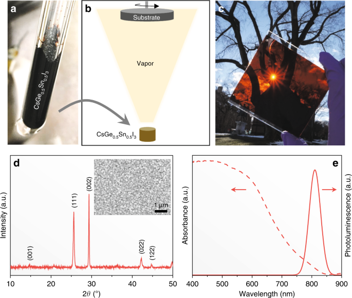
Figure 1(a) is a photograph of CsSn0.5Ge0.5I3 perovskite powder synthesized by solid-state reaction (at 450°C) in an evacuated Pyrex glass tube. The indexed X-ray diffraction pattern (XRD) in Supplementary Fig. 1(a) confirms that this powder is a single-phase perovskite, and it appears to crystallize in the space group of R3m. Its comparison with the XRD pattern of reference CsGeI3 perovskite powder (space group R3m), synthesized using the same procedure, in Supplementary Fig. 1(b) shows peak shifts to lower 2θ angles. This indicates an expansion of the unit cell, as expected with the substitution of the smaller Ge(II) by the larger Sn(II). Reference black phase B-γ-CsSnI3 perovskite, which was also synthesized using the same procedure, crystallizes in the orthorhombic (space group Pnma) structure; Supplementary Fig. 1(c) shows its XRD pattern. (More detailed crystallographic analyses of CsSn1–xGexI3 perovskite alloys will be studied in the future to resolve the symmetry transition with the increase of Ge content.)Figure 1e presents optical absorption and steady-state photoluminescence (PL) spectra of the CsSn0.5Ge0.5I3 perovskite thin film. Good absorption is observed across the visible region, with an edge at about 840 nm, although the estimated Urbach energy is relatively high (37 meV), which could be related to the intrinsic Sn vacancies. The PL emission peak is centered at about 830 nm, which is consistent with the absorption. The PL peak is relatively sharp (FWHM 52 nm), a hallmark of a good light-absorber material. The PL emission was also mapped over a 50 × 50-μm2 area at various locations on the thin films (Supplementary Fig. 3), confirming the optical uniformity across the entire film. The Tauc plot of the thin films in Supplementary Fig. 4a indicates an optical bandgap of about 1.50 eV, which is consistent with that predicted in our earlier computational studies. This bandgap lies in-between the bandgaps of CsSnI3 (1.31 eV) and CsGeI3 (1.63 eV) perovskites, which is to be expected due to the upshift of the valence band maximum (VBM) with the substitution of Sn(II) for Ge(II) in CsGeI3. Supplementary Fig. 4b plots the real and the imaginary parts of the refractive index of the CsSn0.5Ge0.5I3 perovskite thin films as a function of the wavelength.
Native-oxide surface passivation in CsSn0.5Ge0.5I3 perovskite
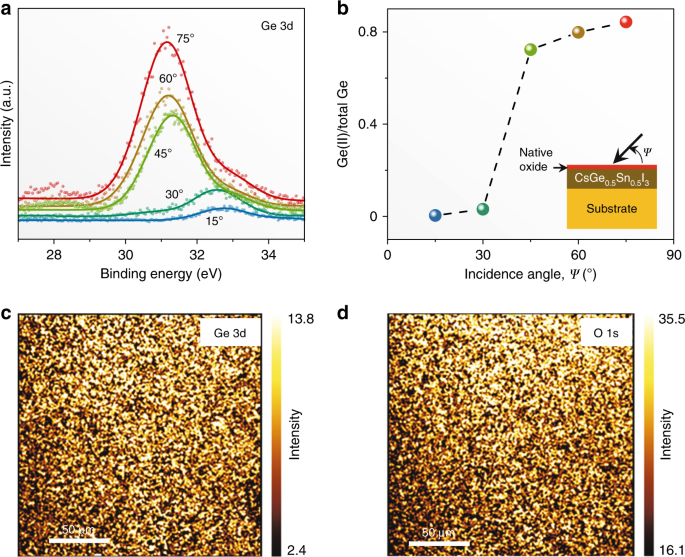
As soon as the CsSn0.5Ge0.5I3 perovskite thin films are exposed to air, a stable native-oxide layer forms on the surface, within 30 s. Figure 2a plots Ge 3d X-ray photoelectron spectroscopy (XPS) spectra at different incidence angles. At shallow angles, the presence of Ge(IV) is detected (binding energy 33.0 eV). Since the surface roughness is about 2.1 nm and the native-oxide layer is expected to be less than 5-nm thick, the surface layer is sampled primarily at such shallow angles. With increasing incidence angle, the Ge(II) peak (binding energy 31.0 eV) dominates, as the underlying CsSn0.5Ge0.5I3 perovskite thin film is sampled primarily. These spectra are deconvoluted, and the estimated Ge(II) content (relative to total Ge) is plotted in Fig. 2b. A sharp drop in the Ge(II) content at incidence angles 30 to 45° indicates a distinct native-oxide layer comprising Ge(IV) primarily. XPS maps (normal incidence angle) of Ge 3d (33.0 eV) and O 1s (532.0 eV) in Fig. 2c, d, respectively, of the same surface region show a strong correlation, confirming the formation of a Ge(IV)-rich native oxide. Supplementary Fig. 5a plots Sn 3d XPS spectra as a function of incidence angle. Since the binding energies for Sn(II) (486.0 eV) and Sn(IV) (486.6 eV) are very close, it is difficult to discern the oxidation state of Sn. Nevertheless, the Sn:Ge atomic ratio is extracted from the data in Supplementary Fig. 5a and Fig. 2a, and it is plotted in Supplementary Fig. 5b as a function of incidence angle. It can be seen that there is a small amount (<10%) of Sn present in the native oxide. In a related experiment, Ar sputtering (15 s) was utilized in situ to remove the native-oxide layer at the surface. The XPS results (15° incidence angle) after Ar sputtering (Supplementary Figs. 6a and 6b) show Ge(II)-rich and O-lean surface corresponding to the CsSn0.5Ge0.5I3 perovskite, which confirms that the thickness of the oxide layer is within 5 nm. Taken together, the XPS results indicate that a uniform layer of Sn-containing Ge(IV)-rich native oxide (<5 nm) forms on the surface of the CsSn0.5Ge0.5I3 perovskite thin films. As with most native-oxide layers that are less than 5 nm in thickness, this native-oxide layer is expected to be amorphous.Native oxide passivated CsSn0.5Ge0.5I3 perovskite stability
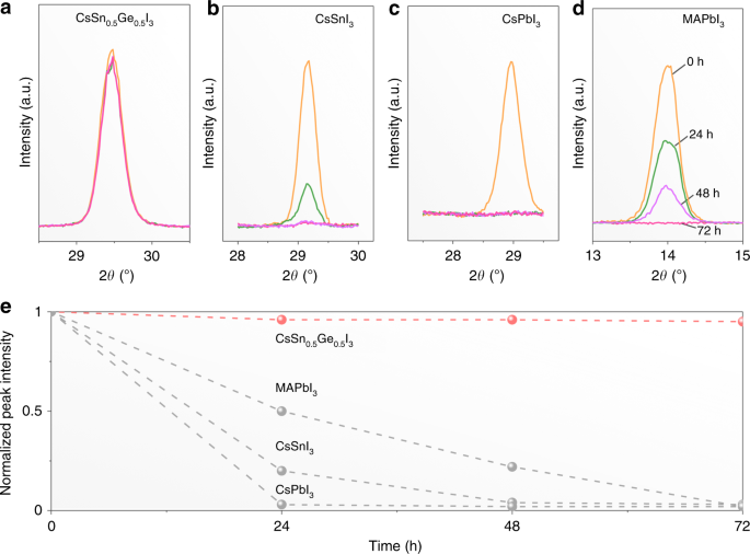
The as-synthesized CsSn0.5Ge0.5I3 perovskite powders when exposed to ambient atmosphere (25 °C, 80% RH) for 24 h remain black and maintain their phase purity (Supplementary Fig. 1d). Moreover, it appears that the CsSnxGe1–xI3 perovskite can become quite stable when the x value is in the range of 0.25–0.75 (Supplementary Fig. 8). In contrast, reference pure CsSnI3 and CsGeI3 powders turn into yellow non-perovskite phases (Supplementary Fig. 1f and 1e). These results demonstrate clearly the superior air stability of the alloy CsSn0.5Ge0.5I3 perovskite over its pure components. The CsSn0.5Ge0.5I3 perovskite thin films subjected to continuous 1-sun illumination in ambient atmosphere (~45 °C, 80% RH) for up to 72 h are also found to be highly stable. Figure 3a presents XRD patterns from CsSn0.5Ge0.5I3 perovskite thin films exposed for 0, 24, 48, and 72 h showing negligible change. The corresponding relative intensities of the main XRD peak are plotted in Fig. 3e. Comparative experiments on thin films of the popular halide perovskites (CsSnI3, CsPbI3, and MAPbI3) show complete degradation after 24, 48, and 72 h, respectively (Fig. 3b–d). Supplementary Fig. 9 presents conductive AFM (c-AFM) images of the CsSn0.5Ge0.5I3 perovskite thin film samples exposed to ambient atmosphere for 0, 24, and 48 h, where the microstructure and conductivity appear unchanged at the nanoscale.Physical properties of CsSn0.5Ge0.5I3 perovskite thin films
The time-resolved PL (TRPL) spectroscopy data from CsSn0.5Ge0.5I3 perovskite thin films (on glass substrates) in Supplementary Fig. 10a reveal a promising lifetime of 10.92 ns, compared with only 510 ps for the reference CsSnI3 thin film. Supplementary Fig. 10b shows TRPL results for CsSn0.5Ge0.5I3 perovskite thin films coated with either phenyl-C61-butyric acid methyl ester:C60 (PCBM:C60) or spiro-OMeTAD as electron- or hole-quenching layers, respectively. Based on the PL decay dynamics, the photogenerated carrier diffusion coefficients are estimated at 0.85 cm2 s−1 and 0.39 cm2 s−1 for electrons and holes, respectively. These correspond to diffusion lengths of 963 nm and 653 nm for electrons and holes, respectively, which are sufficiently long for planar thin-film solar cells.The carrier mobilities in the CsSn0.5Ge0.5I3 perovskite thin films were determined by the space-charge-limited-current (SCLC) method using symmetric capacitor-like devices shown schematically in Supplementary Fig. 11a and 11b insets. For determining the electron mobility (μe) and the hole mobility (μh) in the dark, the Ga/PCBM:C60/CsSn0.5Ge0.5I3/PCBM:C60/Ga and the Au/spiro-OMeTAD/CsSn0.5Ge0.5I3/spiro-OMeTAD/Au device structures, respectively, were used, in conjunction with the following equation:
(1)
Here, JSCL is the measured current density, L is the film thickness (=1 μm), μ is the carrier mobility, ε is the dielectric constant (=28), and εo is the permittivity of free space. The μe and μh are estimated at 974 cm2 V−1 s−1 and 213 cm2 V−1 s−1, respectively, where the latter is consistent with the μh value of 298 cm2 V−1 s−1 determined using the Hall-effect measurements. The electron- and hole-trap densities (nt) were calculated using the following equation:
(2)
Native-oxide-passivated CsSn0.5Ge0.5I3 perovskite solar cells
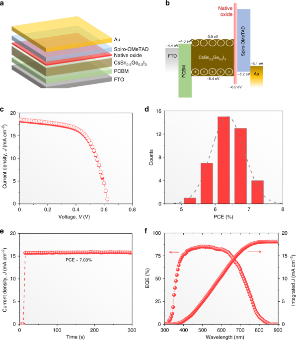
The PV performance of CsSn0.5Ge0.5I3 perovskite thin films with the native-oxide layer is evaluated by incorporating them into PSC devices of the architecture shown in Fig. 4a. The CsSn0.5Ge0.5I3 perovskite thin film (about 200-nm thickness) is sandwiched between PCBM electron-transport layer (ETL) and spiro-OMeTAD hole-transport layer (HTL), with the thin native-oxide layer serving as a wide-bandgap interfacial layer between the CsSn0.5Ge0.5I3 perovskite thin film and the HTL. FTO and Au are used as the conducting electrodes. Figure 4b shows the energy-level diagrams for this device architecture. The VBM and the apparent bandgap of the amorphous native oxide were determined using the ultraviolet photoemission spectroscopy (UPS) results presented in Supplementary Fig. 12. The VBM of the CsSn0.5Ge0.5I3 thin film is determined by performing UPS measurement after the removal of the native-oxide layer using Ar sputtering (Supplementary Fig. 13). Figure 4c plots the current density (J)–voltage (V) responses of the “champion” PSC in reverse and forward scans, showing negligible hysteresis. High overall PCE of 7.11% is achieved with open-circuit voltage (VOC) of 0.63 V, short-circuit current density (JSC) of 18.61 mA cm–2, and fill factor (FF) of 0.606. The JSC value is consistent with the integrated J of 18.1 mA cm–2 from the external quantum efficiency (EQE) spectrum in Fig. 4f. The PCE output at the maximum power point (0.45 V) shows 7.03% in Fig. 4e, which is very close to the extracted PCE from J–V curves. The VOC reported here is much higher than that in other reported PSCs based on all-inorganic Sn-based halide perovskites, and it appears to be stable (Supplementary Fig. 14). The evaluation of PV performance of about 40 PSC devices shows good reproducibility (Fig. 4d), with average PCE of 6.48%. More detailed performance statistics are included in Supplementary Fig. 15, and the device performance parameters are included in Supplementary Table 1.Long-term device stability
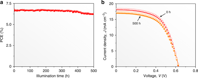
A typical unencapsulated CsSn0.5Ge0.5I3 thin-film PSC with 6.79% PCE (Fig. 5b) was chosen for stability testing where it was operated continuously under continuous 1-sun illumination in N2 atmosphere (45 °C). The continuous monitoring of the PV performance shows that the PCE has degraded to only 6.23% (92% of the initial PCE) after 500 h of continuous operation (Fig. 5a, b). Figure 5b also shows that there is no degradation in the VOC. This demonstrates clearly the excellent operational stability of PSCs based on CsSn0.5Ge0.5I3 perovskite thin films with the native-oxide layer. Regarding the stability in air, we have periodically measured the J–V performance of a CsSn0.5Ge0.5I3-based PSC that was stored under 1-sun illumination. As shown in Supplementary Fig. 18, after 100-h storage, the PSC promisingly maintains 91% of the initial PCE. Overall, to the best of our knowledge, such stability is the highest of all lead-free perovskite PSCs reported so far. Note that, while it is practically challenging to perform a direct performance comparison between the CsSn0.5Ge0.5I3-based and Pb-based PSCs with the same device configuration, the stability of the CsSn0.5Ge0.5I3-based PSCs is reasonably comparable to that of Pb-based PSCs.
To read more, please visit nature.com

0 Comments